

5SGSMD4E2H29I2N
Product Overview
Category
The 5SGSMD4E2H29I2N belongs to the category of Field Programmable Gate Arrays (FPGAs).
Use
This FPGA is designed for high-performance applications that require complex digital logic circuits. It provides a flexible and reconfigurable hardware platform that can be programmed to perform various tasks.
Characteristics
- High-speed processing capabilities
- Large number of configurable logic elements
- On-chip memory resources
- Support for various communication protocols
- Low power consumption
- Scalability for different application requirements
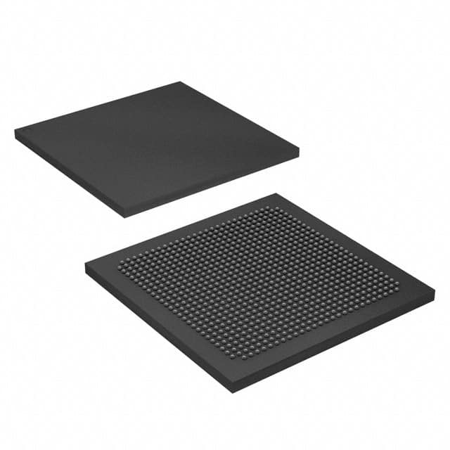
Package
The 5SGSMD4E2H29I2N comes in a compact package that ensures easy integration into electronic systems. The package is designed to provide protection against environmental factors such as temperature, humidity, and electrostatic discharge.
Essence
The essence of the 5SGSMD4E2H29I2N lies in its ability to implement complex digital logic functions using programmable interconnects and configurable logic blocks. This allows designers to create custom hardware solutions without the need for traditional fixed-function integrated circuits.
Packaging/Quantity
The 5SGSMD4E2H29I2N is typically packaged individually and is available in various quantities depending on the specific requirements of the customer or project.
Specifications
- Number of Logic Elements: 5,000
- Number of Embedded Multipliers: 100
- Maximum Operating Frequency: 500 MHz
- On-Chip Memory Capacity: 1,000 KB
- Number of I/O Pins: 200
- Voltage Range: 1.2V - 3.3V
- Package Type: BGA (Ball Grid Array)
- Package Dimensions: 17mm x 17mm
Detailed Pin Configuration
The pin configuration of the 5SGSMD4E2H29I2N is as follows:
- Pin 1: VCCIO
- Pin 2: GND
- Pin 3: CLK_IN
- Pin 4: RESET
- Pin 5: DATA_IN
- Pin 6: DATA_OUT
- Pin 7: ENABLE
- Pin 8: VCC
(Note: This is a simplified representation. The actual pin configuration may include additional pins and functionalities.)
Functional Features
The 5SGSMD4E2H29I2N offers several functional features that enhance its performance and versatility:
- High-speed data processing capabilities
- Support for advanced encryption algorithms
- On-chip memory resources for efficient data storage
- Configurable I/O standards for seamless integration with external devices
- Built-in error detection and correction mechanisms
- Support for partial reconfiguration to enable dynamic hardware updates
Advantages and Disadvantages
Advantages
- Flexibility and reconfigurability for custom hardware designs
- High-performance computing capabilities
- Low power consumption compared to traditional fixed-function integrated circuits
- Scalability to meet varying application requirements
- Support for various communication protocols
Disadvantages
- Steeper learning curve for programming and utilizing FPGA technology
- Higher cost compared to off-the-shelf integrated circuits for simple applications
- Limited availability of specialized technical support for complex designs
Working Principles
The 5SGSMD4E2H29I2N operates based on the principles of digital logic design. It consists of configurable logic blocks, programmable interconnects, and on-chip memory resources. The device can be programmed using Hardware Description Languages (HDL) such as VHDL or Verilog to define the desired functionality. Once programmed, the FPGA executes the specified logic operations, enabling the implementation of complex digital systems.
Detailed Application Field Plans
The 5SGSMD4E2H29I2N finds applications in various fields, including:
- Telecommunications: Used in high-speed data transmission systems and network infrastructure equipment.
- Aerospace and Defense: Employed in radar systems, avionics, and military communication devices.
- Industrial Automation: Utilized for real-time control systems, robotics, and machine vision applications.
- Medical Devices: Integrated into medical imaging systems, patient monitoring devices, and diagnostic equipment.
- Research and Development: Used as a prototyping platform for testing new algorithms and hardware designs.
Detailed and Complete Alternative Models
- 5SGXEA7K2F40C2N: Similar FPGA with higher logic capacity and additional features.
- 5CGXFC9E6F31C7N: Alternative FPGA with lower power consumption and smaller package size.
- 10M08SAU169C8G: Entry-level FPGA with lower logic capacity but more cost-effective for simpler applications.
- 5CEBA4F23C7N: Compact FPGA with moderate logic
10個與5SGSMD4E2H29I2N在技術方案中應用相關的常見問題與解答
Sure! Here are 10 common questions and answers related to the application of 5SGSMD4E2H29I2N in technical solutions:
Q: What is the 5SGSMD4E2H29I2N FPGA used for? A: The 5SGSMD4E2H29I2N is a Field-Programmable Gate Array (FPGA) that can be used for various applications such as high-performance computing, networking, and signal processing.
Q: What are the key features of the 5SGSMD4E2H29I2N FPGA? A: Some key features of this FPGA include high-speed transceivers, large logic capacity, embedded memory blocks, and support for various I/O standards.
Q: Can the 5SGSMD4E2H29I2N FPGA be used for real-time video processing? A: Yes, the FPGA's high-performance capabilities make it suitable for real-time video processing applications like video encoding, decoding, and image recognition.
Q: Is the 5SGSMD4E2H29I2N FPGA suitable for high-frequency trading systems? A: Absolutely, the FPGA's low-latency and high-speed transceivers make it an excellent choice for implementing high-frequency trading algorithms.
Q: Can the 5SGSMD4E2H29I2N FPGA be used for cryptographic applications? A: Yes, the FPGA supports hardware acceleration for cryptographic algorithms, making it ideal for applications like secure communication and data encryption.
Q: Does the 5SGSMD4E2H29I2N FPGA support PCIe connectivity? A: Yes, the FPGA has built-in support for PCIe (Peripheral Component Interconnect Express) connectivity, allowing it to interface with other devices using this standard.
Q: What development tools are available for programming the 5SGSMD4E2H29I2N FPGA? A: The 5SGSMD4E2H29I2N FPGA can be programmed using popular development tools like Quartus Prime from Intel (formerly Altera).
Q: Can the 5SGSMD4E2H29I2N FPGA be used in safety-critical applications? A: Yes, the FPGA supports various safety features like error detection and correction, making it suitable for safety-critical applications such as aerospace or automotive systems.
Q: Is the 5SGSMD4E2H29I2N FPGA compatible with industry-standard interfaces? A: Yes, the FPGA supports a wide range of industry-standard interfaces like Ethernet, USB, HDMI, and more, making it easy to integrate into existing systems.
Q: Are there any reference designs or application notes available for the 5SGSMD4E2H29I2N FPGA? A: Yes, Intel provides a comprehensive set of reference designs, application notes, and documentation to help developers get started with the 5SGSMD4E2H29I2N FPGA and its various applications.
Please note that the specific details and answers may vary depending on the context and requirements of the technical solution.