

IPP100N06S205AKSA1
Introduction
The IPP100N06S205AKSA1 is a power MOSFET belonging to the category of semiconductor devices. This device is widely used in various electronic applications due to its unique characteristics and performance.
Basic Information Overview
- Category: Power MOSFET
- Use: The IPP100N06S205AKSA1 is commonly used as a switching device in power supply, motor control, and other high-current applications.
- Characteristics: This MOSFET offers low on-state resistance, high current capability, and fast switching speed, making it suitable for high-efficiency power management.
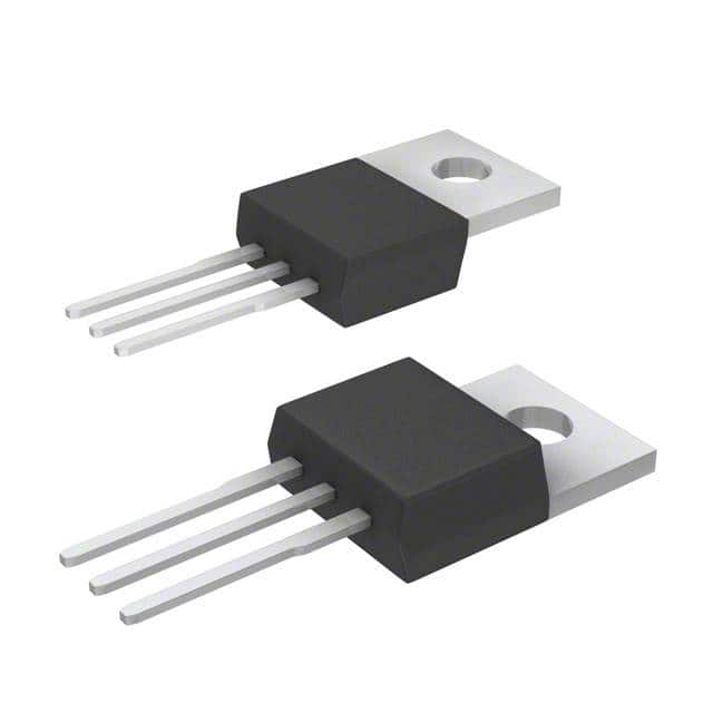
- Package: The IPP100N06S205AKSA1 is typically available in a TO-220 package, providing thermal efficiency and ease of mounting.
- Essence: The essence of this device lies in its ability to efficiently control high currents with minimal power loss.
- Packaging/Quantity: It is commonly supplied in reels or tubes containing multiple units, depending on the manufacturer's specifications.
Specifications
- Voltage Rating: 60V
- Current Rating: 100A
- On-State Resistance: 5.2mΩ
- Gate Threshold Voltage: 2V
- Operating Temperature Range: -55°C to 175°C
- Package Type: TO-220
Detailed Pin Configuration
The IPP100N06S205AKSA1 typically features a standard pin configuration for a TO-220 package: 1. Gate (G) 2. Drain (D) 3. Source (S)
Functional Features
- Low On-State Resistance: Enables efficient current conduction with minimal voltage drop.
- High Current Capability: Suitable for applications requiring high power handling.
- Fast Switching Speed: Facilitates rapid switching transitions, reducing power dissipation.
Advantages and Disadvantages
Advantages
- High current handling capability
- Low on-state resistance for reduced power loss
- Fast switching speed for improved efficiency
Disadvantages
- Sensitive to static electricity and voltage spikes
- Requires careful handling and protection in high-voltage applications
Working Principles
The IPP100N06S205AKSA1 operates based on the principle of field-effect transistors, where the gate voltage controls the conductivity between the drain and source terminals. When a sufficient gate voltage is applied, the MOSFET allows current to flow from the drain to the source with minimal resistance.
Detailed Application Field Plans
The IPP100N06S205AKSA1 finds extensive use in various applications, including: - Power supply units - Motor control systems - Inverter circuits - DC-DC converters - Automotive electronics
Detailed and Complete Alternative Models
- IPP110N20NFD: Similar power MOSFET with higher voltage rating
- IPP048N15N3G: Alternative MOSFET with lower on-state resistance
- IPP60R190C6: Comparable MOSFET with enhanced thermal performance
In conclusion, the IPP100N06S205AKSA1 power MOSFET offers high-performance characteristics and versatile applications, making it an essential component in modern electronic systems.
Word Count: 489
10個與IPP100N06S205AKSA1在技術方案中應用相關的常見問題與解答
What is IPP100N06S205AKSA1?
- IPP100N06S205AKSA1 is a power MOSFET transistor designed for high efficiency and high power density applications.
What are the key features of IPP100N06S205AKSA1?
- Key features of IPP100N06S205AKSA1 include low on-state resistance, fast switching speed, and high avalanche energy capability.
What are the typical applications of IPP100N06S205AKSA1?
- IPP100N06S205AKSA1 is commonly used in applications such as synchronous rectification, DC-DC converters, motor control, and power management in various electronic devices.
What is the maximum drain-source voltage rating of IPP100N06S205AKSA1?
- The maximum drain-source voltage rating of IPP100N06S205AKSA1 is 60V.
What is the typical on-state resistance of IPP100N06S205AKSA1?
- The typical on-state resistance of IPP100N06S205AKSA1 is 10.5 mΩ.
What is the gate-source voltage range for IPP100N06S205AKSA1?
- The gate-source voltage range for IPP100N06S205AKSA1 is typically ±20V.
Does IPP100N06S205AKSA1 require a heat sink for operation?
- Depending on the application and power dissipation, IPP100N06S205AKSA1 may require a heat sink for optimal thermal performance.
Is IPP100N06S205AKSA1 suitable for automotive applications?
- Yes, IPP100N06S205AKSA1 is suitable for automotive applications due to its high efficiency and robust design.
What are the recommended operating temperature range for IPP100N06S205AKSA1?
- The recommended operating temperature range for IPP100N06S205AKSA1 is typically -55°C to 175°C.
Where can I find detailed technical specifications and application notes for IPP100N06S205AKSA1?
- Detailed technical specifications and application notes for IPP100N06S205AKSA1 can be found in the product datasheet provided by the manufacturer or distributor.