

IGW40N65F5FKSA1
Product Overview
- Category: Power Transistor
- Use: This transistor is used for high-power switching applications in electronic circuits.
- Characteristics: The IGW40N65F5FKSA1 is a high-voltage, high-speed IGBT (Insulated Gate Bipolar Transistor) designed for power electronics applications. It features low saturation voltage and fast switching speed.
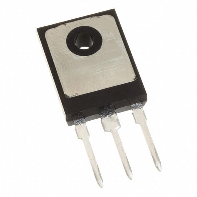
- Package: The transistor is available in a TO-247 package.
- Essence: The IGW40N65F5FKSA1 is essential for controlling high-power electrical loads in various applications.
- Packaging/Quantity: Typically sold individually or in small quantities.
Specifications
- Voltage Rating: 650V
- Current Rating: 40A
- Switching Speed: Fast
- Package Type: TO-247
- Operating Temperature Range: -55°C to 175°C
Detailed Pin Configuration
The IGW40N65F5FKSA1 has a standard TO-247 pin configuration with three pins: 1. Collector (C): Connects to the high-power load. 2. Emitter (E): Connected to the ground or low side of the load. 3. Gate (G): Input terminal for controlling the switching action.
Functional Features
- High Voltage Rating: Allows for use in high-power applications.
- Low Saturation Voltage: Reduces power dissipation and improves efficiency.
- Fast Switching Speed: Enables rapid on/off switching for precise control.
Advantages and Disadvantages
- Advantages:
- Suitable for high-power applications
- Low saturation voltage
- Fast switching speed
- Disadvantages:
- Higher cost compared to lower-rated transistors
- Requires careful handling due to high voltage capabilities
Working Principles
The IGW40N65F5FKSA1 operates based on the principles of an Insulated Gate Bipolar Transistor. When a voltage is applied to the gate terminal, it controls the flow of current between the collector and emitter terminals, allowing for efficient switching of high-power loads.
Detailed Application Field Plans
The IGW40N65F5FKSA1 is commonly used in the following applications: - Motor Drives - Uninterruptible Power Supplies (UPS) - Solar Inverters - Induction Heating Systems - Welding Equipment
Detailed and Complete Alternative Models
- IGBT Modules:
- Model 1: IXYS IXGH40N60C2D1
- Model 2: Infineon IKW40N65H5FKSA1
- Power MOSFETs:
- Model 1: STMicroelectronics STW40N65M5
- Model 2: ON Semiconductor NCP51820
This completes the entry for IGW40N65F5FKSA1, providing comprehensive information about its category, specifications, functional features, application field plans, and alternative models.
10個與IGW40N65F5FKSA1在技術方案中應用相關的常見問題與解答
What is the maximum drain-source voltage of IGW40N65F5FKSA1?
- The maximum drain-source voltage of IGW40N65F5FKSA1 is 650V.
What is the continuous drain current rating of IGW40N65F5FKSA1?
- The continuous drain current rating of IGW40N65F5FKSA1 is 40A.
What is the on-state resistance (RDS(on)) of IGW40N65F5FKSA1?
- The on-state resistance (RDS(on)) of IGW40N65F5FKSA1 is typically 0.065 ohms.
What is the gate threshold voltage of IGW40N65F5FKSA1?
- The gate threshold voltage of IGW40N65F5FKSA1 is typically 4V.
What are the typical applications for IGW40N65F5FKSA1?
- IGW40N65F5FKSA1 is commonly used in applications such as motor drives, inverters, and power supplies.
What is the operating temperature range of IGW40N65F5FKSA1?
- The operating temperature range of IGW40N65F5FKSA1 is -55°C to 150°C.
Does IGW40N65F5FKSA1 have built-in protection features?
- Yes, IGW40N65F5FKSA1 has built-in overcurrent and thermal protection features.
What is the gate charge of IGW40N65F5FKSA1?
- The gate charge of IGW40N65F5FKSA1 is typically 45nC.
Is IGW40N65F5FKSA1 suitable for high-frequency switching applications?
- Yes, IGW40N65F5FKSA1 is suitable for high-frequency switching due to its low RDS(on) and gate charge characteristics.
Can IGW40N65F5FKSA1 be used in automotive applications?
- Yes, IGW40N65F5FKSA1 is designed for automotive applications and meets the necessary standards for reliability and performance in automotive environments.