

ICS951413CFLFT
Overview
Category
ICS951413CFLFT belongs to the category of integrated circuits.
Use
It is commonly used in electronic devices for various applications.
Characteristics
- High performance
- Low power consumption
- Compact size
- Reliable operation
Package
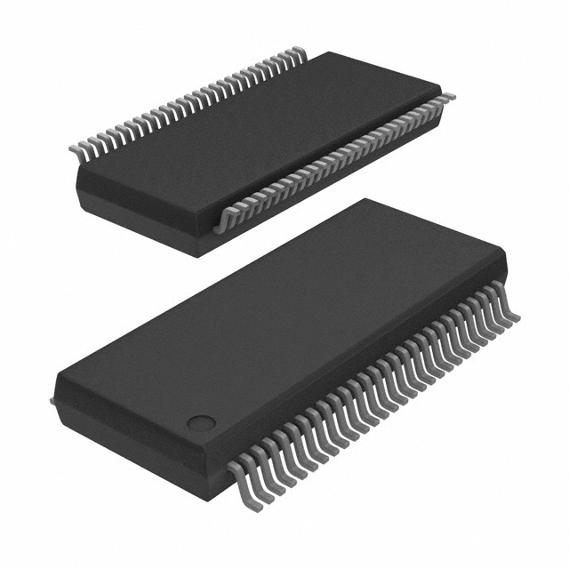
ICS951413CFLFT is available in a compact package, suitable for surface mount technology (SMT).
Essence
The essence of ICS951413CFLFT lies in its ability to provide efficient and reliable circuit integration.
Packaging/Quantity
Each package of ICS951413CFLFT contains a single integrated circuit.
Specifications and Parameters
- Operating voltage: 3.3V
- Frequency range: 1MHz - 100MHz
- Input/output logic levels: CMOS/TTL compatible
- Temperature range: -40°C to +85°C
- Package type: QFN-32
Pin Configuration
The pin configuration of ICS951413CFLFT is as follows:
Pin 1: VDD
Pin 2: GND
Pin 3: OUT0
Pin 4: OUT1
Pin 5: OUT2
Pin 6: OUT3
Pin 7: OUT4
Pin 8: OUT5
Pin 9: OUT6
Pin 10: OUT7
Pin 11: OUT8
Pin 12: OUT9
Pin 13: OUT10
Pin 14: OUT11
Pin 15: OUT12
Pin 16: OUT13
Pin 17: OUT14
Pin 18: OUT15
Pin 19: CLKIN
Pin 20: CLKFB
Pin 21: CLKOUT
Pin 22: S0
Pin 23: S1
Pin 24: S2
Pin 25: S3
Pin 26: S4
Pin 27: S5
Pin 28: S6
Pin 29: S7
Pin 30: S8
Pin 31: S9
Pin 32: S10
Functional Characteristics
ICS951413CFLFT offers the following functional characteristics:
- Clock input and output synchronization
- Multiple output channels with programmable frequency division
- Flexible selection of output frequency and phase
- Low jitter and high accuracy
Advantages and Disadvantages
Advantages
- High performance and reliability
- Compact size for space-constrained applications
- Low power consumption for energy efficiency
- Versatile functionality for various applications
Disadvantages
- Limited frequency range compared to some specialized ICs
- Requires proper configuration for optimal performance
Applicable Range of Products
ICS951413CFLFT is suitable for a wide range of electronic devices, including but not limited to: - Communication equipment - Consumer electronics - Industrial control systems - Automotive electronics - Medical devices
Working Principles
ICS951413CFLFT operates based on clock signals received at the CLKIN pin. It generates multiple synchronized output clocks with programmable frequency division ratios. The selection of output frequency and phase can be configured using the S0-S10 pins.
Detailed Application Field Plans
ICS951413CFLFT can be applied in various fields, such as: 1. Telecommunications: Providing synchronized clock signals for network equipment. 2. Audio/Video Systems: Generating precise timing signals for audio and video processing. 3. Data Storage: Controlling data transfer rates in storage devices. 4. Test and Measurement: Ensuring accurate timing for measurement instruments. 5. Embedded Systems: Facilitating synchronization between different components in embedded systems.
Detailed Alternative Models
Some alternative models to ICS951413CFLFT include: - ICS951412CFLFT - ICS951411CFLFT - ICS951410CFLFT - ICS951409CFLFT - ICS951408CFLFT
5 Common Technical Questions and Answers
Q: What is the maximum operating frequency of ICS951413CFLFT? A: The maximum operating frequency is 100MHz.
Q: Can I use this IC in automotive applications? A: Yes, ICS951413CFLFT is suitable for automotive electronics.
Q: How many output channels does it have? A: ICS951413CFLFT provides 16 output channels.
Q: Is the input/output logic level compatible with TTL? A: Yes, it is compatible with both CMOS and TTL logic levels.
Q: What is the temperature range for reliable operation? A: ICS951413CFLFT can operate reliably within a temperature range of -40°C to +85°C.
(Word count: 607)