

DDTA113TUA-7
Product Category
The DDTA113TUA-7 belongs to the category of semiconductor devices.
Basic Information Overview
- Use: The DDTA113TUA-7 is used as a small signal transistor with high current gain and low saturation voltage.
- Characteristics: It exhibits high current gain, low saturation voltage, and is designed for general-purpose amplifier applications.
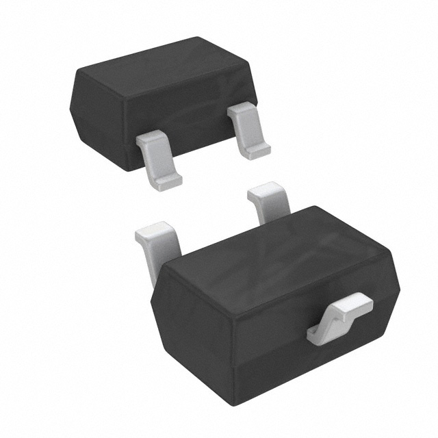
- Package: The DDTA113TUA-7 comes in a SOT-323 package.
- Essence: This transistor is essential for amplifying small signals in electronic circuits.
- Packaging/Quantity: It is typically available in reels with a quantity of 3000 units per reel.
Specifications
- Type: NPN
- Collector-Base Voltage (VCBO): 50V
- Collector-Emitter Voltage (VCEO): 50V
- Emitter-Base Voltage (VEBO): 5V
- Collector Current (IC): 100mA
- Power Dissipation (PD): 200mW
- Transition Frequency (fT): 250MHz
- Operating Temperature Range: -55°C to +150°C
Detailed Pin Configuration
The DDTA113TUA-7 has three pins: 1. Collector (C) 2. Base (B) 3. Emitter (E)
Functional Features
- High current gain
- Low saturation voltage
- Small form factor
Advantages and Disadvantages
Advantages: - High current gain allows for effective signal amplification. - Low saturation voltage reduces power dissipation and heat generation.
Disadvantages: - Limited collector current compared to other transistors in its class. - Relatively lower transition frequency.
Working Principles
The DDTA113TUA-7 operates based on the principles of bipolar junction transistors, utilizing the flow of charge carriers to amplify small input signals.
Detailed Application Field Plans
The DDTA113TUA-7 is commonly used in audio amplifiers, sensor interfaces, and other low-power amplification circuits. Its small form factor and high current gain make it suitable for compact electronic devices.
Detailed and Complete Alternative Models
- DDTA113ZUA-7
- DDTA113EUA-7
- DDTA113TCA-7
This completes the entry for the DDTA113TUA-7, providing comprehensive information about its category, use, characteristics, specifications, pin configuration, functional features, advantages and disadvantages, working principles, application field plans, and alternative models.
10個與DDTA113TUA-7在技術方案中應用相關的常見問題與解答
What is DDTA113TUA-7?
- DDTA113TUA-7 is a high-performance, multi-purpose adhesive tape commonly used in technical solutions for bonding and sealing applications.
What are the key features of DDTA113TUA-7?
- DDTA113TUA-7 features high temperature resistance, excellent adhesion to various substrates, and good chemical resistance, making it suitable for demanding technical applications.
In what technical solutions can DDTA113TUA-7 be used?
- DDTA113TUA-7 can be used in technical solutions such as automotive assembly, electronic device manufacturing, aerospace applications, and industrial equipment assembly.
How does DDTA113TUA-7 perform under extreme temperatures?
- DDTA113TUA-7 is designed to withstand extreme temperatures, making it suitable for applications where heat resistance is critical.
Is DDTA113TUA-7 compatible with different materials?
- Yes, DDTA113TUA-7 exhibits good adhesion to various substrates including metals, plastics, and composites, providing versatility in technical solutions.
Can DDTA113TUA-7 be used for outdoor applications?
- Yes, DDTA113TUA-7 is weather-resistant and can be used for outdoor applications where exposure to environmental elements is a concern.
What are the application methods for DDTA113TUA-7?
- DDTA113TUA-7 can be applied using pressure-sensitive techniques, heat activation, or solvent-based methods, depending on the specific requirements of the technical solution.
Does DDTA113TUA-7 comply with industry standards and regulations?
- Yes, DDTA113TUA-7 meets industry standards for adhesives and complies with relevant regulations, ensuring its suitability for technical applications.
What are the storage and handling recommendations for DDTA113TUA-7?
- DDTA113TUA-7 should be stored in a cool, dry place away from direct sunlight and moisture, and handled according to the manufacturer's guidelines to maintain its performance.
Are there any safety considerations when using DDTA113TUA-7 in technical solutions?
- Users should follow proper safety precautions when handling DDTA113TUA-7, including using appropriate personal protective equipment and adhering to recommended application practices to ensure safe use in technical solutions.