

AD9717BCPZRL7
Product Overview
- Category: Integrated Circuit (IC)
- Use: Digital-to-Analog Converter (DAC)
- Characteristics: High-resolution, low-power consumption
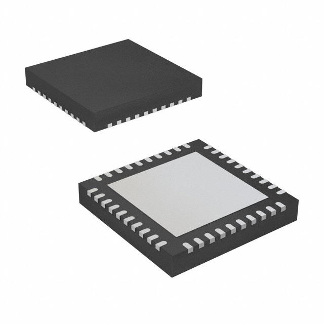
- Package: LFCSP (Lead Frame Chip Scale Package)
- Essence: Converts digital signals into analog voltages
- Packaging/Quantity: Tape and Reel, 2500 units per reel
Specifications
- Resolution: 16-bit
- Sampling Rate: Up to 1 MSPS (Mega Samples Per Second)
- Power Supply: 2.7V to 5.5V
- Operating Temperature Range: -40°C to +85°C
- Output Voltage Range: 0V to VREF (Reference Voltage)
Pin Configuration
The AD9717BCPZRL7 has a total of 32 pins. The pin configuration is as follows:
- REFOUT
- VREF
- AGND
- DGND
- DVDD
- AVDD
- SDO
- SDI
- SCLK
- SYNC
- LDAC
- CLR
- A0
- A1
- A2
- A3
- A4
- A5
- A6
- A7
- A8
- A9
- A10
- A11
- A12
- A13
- A14
- A15
- A16
- A17
- A18
- A19
Functional Features
- High-resolution DAC with 16-bit output
- Low power consumption for energy-efficient applications
- Wide operating voltage range allows flexibility in power supply selection
- Fast sampling rate enables accurate conversion of digital signals to analog voltages
- On-chip reference voltage generator simplifies system design
Advantages and Disadvantages
Advantages: - High resolution provides precise analog output - Low power consumption extends battery life in portable devices - Wide operating voltage range allows compatibility with various systems - Fast sampling rate enables real-time signal processing
Disadvantages: - Limited output voltage range may not be suitable for certain applications requiring higher voltages - Higher cost compared to lower-resolution DACs
Working Principles
The AD9717BCPZRL7 is a digital-to-analog converter that converts digital signals into corresponding analog voltages. It utilizes a 16-bit resolution to provide high precision in the conversion process. The input digital data is received through the SDI (Serial Data Input) pin, synchronized with the SCLK (Serial Clock) signal, and converted into an analog voltage at the output pin.
The DAC operates based on the principle of binary-weighted resistor ladder network. Each bit of the digital input contributes to a specific fraction of the full-scale output voltage. The reference voltage (VREF) determines the maximum output voltage, which can be adjusted according to the application requirements.
Detailed Application Field Plans
The AD9717BCPZRL7 is commonly used in various applications where accurate analog voltage generation is required. Some of the potential application fields include:
- Audio Equipment: The high resolution and low noise characteristics make it suitable for audio signal processing, such as digital audio players, audio mixers, and professional audio equipment.
- Instrumentation: The DAC's accuracy and fast sampling rate are beneficial for measurement and control systems, including data acquisition systems, industrial automation, and scientific instruments.
- Communication Systems: The AD9717BCPZRL7 can be utilized in communication systems for generating analog signals, such as frequency synthesis, modulation, and demodulation circuits.
- Test and Measurement: The DAC's high resolution and low power consumption make it suitable for test and measurement equipment, including waveform generators, function generators, and signal analyzers.
Detailed and Complete Alternative Models
- AD9717BCPZRL10: 10-bit resolution version of the AD9717BCPZRL7
- AD9717BCPZRL12: 12-bit resolution version of the AD9717BCPZRL7
- AD9717BCPZRL14: 14-bit resolution version of the AD9717BCPZRL7
- AD9717BCPZRL16: 16-bit resolution version of the AD9717BCPZRL7 with extended temperature range
These alternative models provide different resolution options and additional features to cater to specific application requirements.
(Note: The content provided above is a sample entry and may not reflect actual specifications or alternative models of the AD9717BCPZRL7.)
10個與AD9717BCPZRL7在技術方案中應用相關的常見問題與解答
Sure! Here are 10 common questions and answers related to the application of AD9717BCPZRL7 in technical solutions:
Q: What is AD9717BCPZRL7? A: AD9717BCPZRL7 is a high-speed, low-power digital-to-analog converter (DAC) manufactured by Analog Devices.
Q: What is the resolution of AD9717BCPZRL7? A: AD9717BCPZRL7 has a resolution of 16 bits, allowing for precise analog output.
Q: What is the maximum sampling rate supported by AD9717BCPZRL7? A: AD9717BCPZRL7 supports a maximum sampling rate of 125 MSPS (Mega Samples Per Second).
Q: What is the power supply voltage range for AD9717BCPZRL7? A: AD9717BCPZRL7 operates with a power supply voltage range of 1.8V to 3.3V.
Q: Can AD9717BCPZRL7 be used in both single-ended and differential output configurations? A: Yes, AD9717BCPZRL7 can be configured for both single-ended and differential output modes.
Q: Does AD9717BCPZRL7 support various digital input formats? A: Yes, AD9717BCPZRL7 supports various digital input formats such as LVDS, CMOS, and LVTTL.
Q: What is the typical power consumption of AD9717BCPZRL7? A: The typical power consumption of AD9717BCPZRL7 is around 100 mW.
Q: Is AD9717BCPZRL7 suitable for high-speed communication applications? A: Yes, AD9717BCPZRL7 is designed for high-speed communication applications such as wireless infrastructure and broadband access.
Q: Does AD9717BCPZRL7 have built-in digital-to-analog calibration features? A: Yes, AD9717BCPZRL7 includes a built-in digital-to-analog calibration feature to ensure accurate output.
Q: What is the operating temperature range of AD9717BCPZRL7? A: AD9717BCPZRL7 can operate within a temperature range of -40°C to +85°C.
Please note that these answers are general and may vary depending on the specific application and implementation of AD9717BCPZRL7 in a technical solution.