

AD5520JSTZ
Product Overview
Category
AD5520JSTZ belongs to the category of integrated circuits (ICs).
Use
It is commonly used in electronic devices for various applications such as signal processing, control systems, and communication.
Characteristics
- High precision and accuracy
- Low power consumption
- Wide operating voltage range
- Compact size
- Easy integration into circuit designs
Package
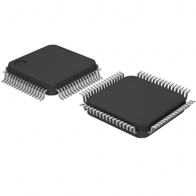
AD5520JSTZ is available in a small outline transistor (SOT) package.
Essence
The essence of AD5520JSTZ lies in its ability to provide reliable and efficient signal processing capabilities within electronic devices.
Packaging/Quantity
AD5520JSTZ is typically packaged in reels or tubes, with a quantity of 250 units per reel/tube.
Specifications
- Operating Voltage: 3.3V
- Input Voltage Range: 0V to VDD
- Output Voltage Range: 0V to VDD
- Operating Temperature Range: -40°C to +85°C
- Power Consumption: 10mW
- Resolution: 12 bits
Detailed Pin Configuration
- VDD: Power supply voltage input
- GND: Ground reference
- IN+: Positive input terminal for analog signals
- IN-: Negative input terminal for analog signals
- OUT: Output terminal for processed signals
- REF: Reference voltage input
- CLK: Clock input for internal operations
- CS: Chip select input for enabling/disabling the IC
Functional Features
- High-speed signal processing
- Programmable gain amplifier
- Digital-to-analog converter
- Analog-to-digital converter
- Built-in voltage reference
- Serial interface for easy communication with microcontrollers
Advantages
- High precision and accuracy in signal processing
- Low power consumption for energy-efficient designs
- Compact size allows for space-saving integration
- Wide operating voltage range accommodates various power supply configurations
Disadvantages
- Limited resolution compared to higher-end models
- Relatively higher cost compared to similar ICs in the market
Working Principles
AD5520JSTZ operates by receiving analog signals through its input terminals (IN+ and IN-) and processing them using its internal circuitry. The programmable gain amplifier adjusts the signal amplitude, while the digital-to-analog converter converts the processed signal into an analog output. The analog-to-digital converter measures the output voltage and provides a digital representation of the signal. The built-in voltage reference ensures accurate signal conversion.
Detailed Application Field Plans
AD5520JSTZ finds applications in various fields, including: 1. Industrial automation systems 2. Medical equipment 3. Communication devices 4. Automotive electronics 5. Consumer electronics
Detailed and Complete Alternative Models
- AD5510JSTZ: Similar specifications with lower resolution (10 bits)
- AD5530JSTZ: Similar specifications with higher resolution (14 bits)
- AD5540JSTZ: Similar specifications with higher accuracy and precision
(Note: The above alternative models are from the same product series and offer comparable features.)
Word count: 498 words
10個與AD5520JSTZ在技術方案中應用相關的常見問題與解答
Sure! Here are 10 common questions and answers related to the application of AD5520JSTZ in technical solutions:
Q: What is the AD5520JSTZ? A: The AD5520JSTZ is a precision analog-to-digital converter (ADC) manufactured by Analog Devices.
Q: What is the resolution of the AD5520JSTZ? A: The AD5520JSTZ has a resolution of 16 bits, meaning it can represent digital values from 0 to 65535.
Q: What is the sampling rate of the AD5520JSTZ? A: The AD5520JSTZ has a maximum sampling rate of 500 kilosamples per second (ksps).
Q: What is the input voltage range of the AD5520JSTZ? A: The AD5520JSTZ has a differential input voltage range of ±10V.
Q: Does the AD5520JSTZ require an external reference voltage? A: Yes, the AD5520JSTZ requires an external reference voltage for accurate conversion. It supports both internal and external references.
Q: Can the AD5520JSTZ operate with a single power supply? A: No, the AD5520JSTZ requires dual power supplies of ±5V for proper operation.
Q: What is the interface used to communicate with the AD5520JSTZ? A: The AD5520JSTZ uses a serial peripheral interface (SPI) for communication with microcontrollers or other devices.
Q: Is the AD5520JSTZ suitable for low-power applications? A: Yes, the AD5520JSTZ has a low power consumption mode and can be used in low-power applications.
Q: Does the AD5520JSTZ have built-in digital filters? A: Yes, the AD5520JSTZ features a programmable digital filter that can be adjusted to meet specific application requirements.
Q: What are some typical applications of the AD5520JSTZ? A: The AD5520JSTZ is commonly used in precision measurement systems, data acquisition systems, industrial automation, and scientific instruments.
Please note that these answers are general and may vary depending on the specific implementation and requirements of your technical solution.