

AD5323BRU
Product Overview
- Category: Integrated Circuit (IC)
- Use: Digital-to-Analog Converter (DAC)
- Characteristics: High-resolution, low-power consumption
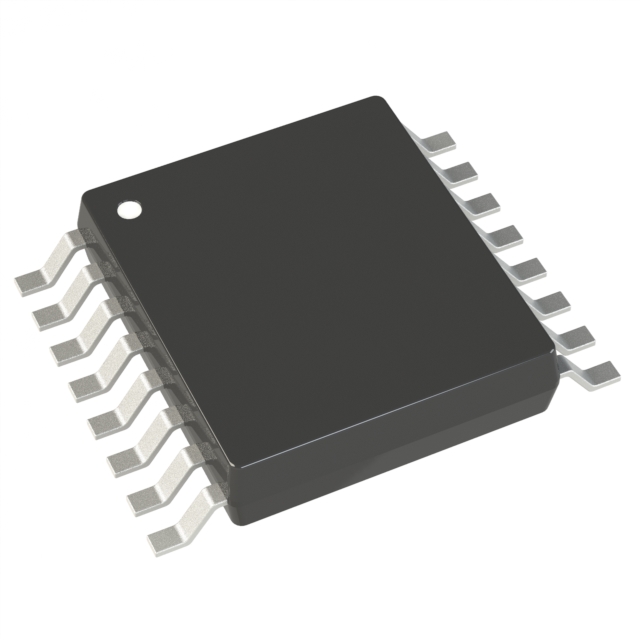
- Package: 16-pin TSSOP (Thin Shrink Small Outline Package)
- Essence: Converts digital signals into analog voltages
- Packaging/Quantity: Available in reels of 2500 units
Specifications
- Resolution: 12 bits
- Number of Channels: 8
- Supply Voltage Range: 2.7V to 5.5V
- Operating Temperature Range: -40°C to +105°C
- Output Voltage Range: 0V to Vref (Reference Voltage)
- Power Consumption: 0.6mW at 3V supply voltage
Detailed Pin Configuration
The AD5323BRU has a total of 16 pins, which are assigned as follows:
- VDD: Positive power supply
- VREF: Reference voltage input
- AGND: Analog ground
- AOUT0: Analog output channel 0
- AOUT1: Analog output channel 1
- AOUT2: Analog output channel 2
- AOUT3: Analog output channel 3
- AOUT4: Analog output channel 4
- AOUT5: Analog output channel 5
- AOUT6: Analog output channel 6
- AOUT7: Analog output channel 7
- DGND: Digital ground
- DIN: Serial data input
- SCLK: Serial clock input
- SYNC: Serial interface synchronization input
- CS: Chip select input
Functional Features
- High-resolution DAC with 12-bit resolution
- Low-power consumption for energy-efficient applications
- Serial interface for easy integration with microcontrollers and digital systems
- Wide supply voltage range allows for flexibility in power source selection
- Output voltage range can be adjusted according to the reference voltage
Advantages and Disadvantages
Advantages: - High resolution provides precise analog output - Low-power consumption extends battery life in portable devices - Serial interface simplifies communication with other digital components - Wide supply voltage range enhances compatibility with various systems
Disadvantages: - Limited number of channels (8) - Requires an external reference voltage for accurate conversion
Working Principles
The AD5323BRU is a digital-to-analog converter that converts digital signals into corresponding analog voltages. It utilizes a 12-bit resolution to provide high precision in the conversion process. The input digital data is received through the serial interface, and the internal circuitry converts it into an analog voltage based on the reference voltage provided. The converted analog voltage is then available at the respective analog output channel pins.
Detailed Application Field Plans
The AD5323BRU is commonly used in various applications that require digital-to-analog conversion. Some potential application fields include:
- Audio Systems: Used to convert digital audio signals into analog signals for amplification and playback.
- Industrial Automation: Utilized in control systems to generate analog control signals for actuators and sensors.
- Test and Measurement Equipment: Employed to generate precise analog test signals for calibration and testing purposes.
- Communication Systems: Integrated into transceivers to convert digital baseband signals into analog signals for transmission.
Detailed and Complete Alternative Models
- AD5300BRUZ: 8-bit resolution DAC with similar pin configuration and package.
- AD5620BRJZ-2500RL7: 12-bit resolution DAC with SPI interface and different package.
- AD5660ARJZ-2500RL7: 16-bit resolution DAC with similar pin configuration and package.
These alternative models offer different resolutions, interfaces, and package options to cater to specific application requirements.
Word count: 409 words
10個與AD5323BRU在技術方案中應用相關的常見問題與解答
Sure! Here are 10 common questions and answers related to the application of AD5323BRU in technical solutions:
Q: What is the AD5323BRU? A: The AD5323BRU is a digital-to-analog converter (DAC) chip manufactured by Analog Devices.
Q: What is the resolution of the AD5323BRU? A: The AD5323BRU has a resolution of 12 bits, allowing for precise analog output control.
Q: What is the voltage range of the AD5323BRU? A: The AD5323BRU operates with a voltage range of 0V to Vref, where Vref is the reference voltage supplied to the chip.
Q: How many channels does the AD5323BRU have? A: The AD5323BRU has 8 independent channels, each capable of generating an analog output voltage.
Q: Can the AD5323BRU be controlled digitally? A: Yes, the AD5323BRU can be controlled via a serial interface using standard protocols such as SPI or I2C.
Q: What is the power supply requirement for the AD5323BRU? A: The AD5323BRU requires a single power supply voltage ranging from 2.7V to 5.5V.
Q: Is the AD5323BRU suitable for precision applications? A: Yes, the AD5323BRU offers excellent linearity and low integral nonlinearity, making it suitable for precision applications.
Q: Can the AD5323BRU operate in a low-power mode? A: Yes, the AD5323BRU features a power-down mode that reduces power consumption when the device is not in use.
Q: What is the settling time of the AD5323BRU? A: The settling time of the AD5323BRU is typically 10 μs, ensuring fast and accurate output voltage transitions.
Q: Can the AD5323BRU be used in industrial applications? A: Yes, the AD5323BRU is designed to operate reliably in harsh industrial environments, making it suitable for various industrial applications.
Please note that these answers are general and may vary depending on specific implementation details and requirements.