

ALD1701APAL
Product Overview
Category: Integrated Circuit (IC)
Use: The ALD1701APAL is a versatile integrated circuit designed for various applications in electronic devices. It offers precise control and measurement capabilities, making it suitable for use in a wide range of electronic systems.
Characteristics: - High precision - Low power consumption - Compact size - Wide operating voltage range
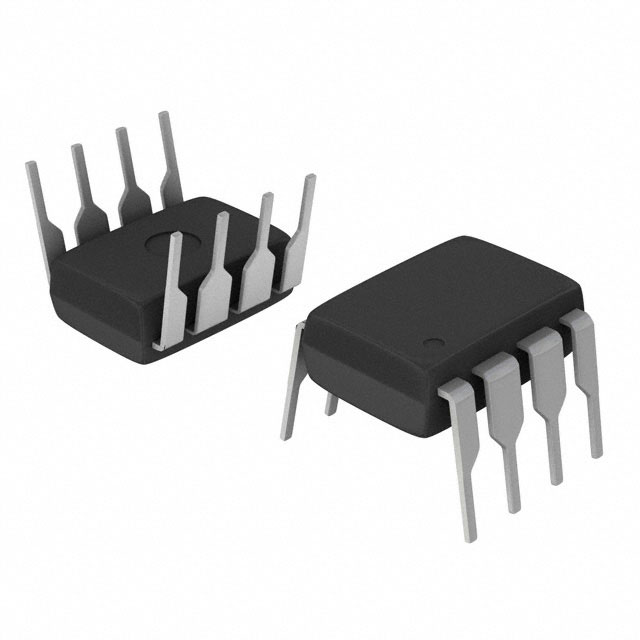
Package: The ALD1701APAL is available in a small outline package (SOP) which ensures easy integration into electronic circuits.
Essence: This IC serves as a key component in electronic systems, providing accurate control and measurement functions.
Packaging/Quantity: The ALD1701APAL is typically sold in reels or tubes, with each reel/tube containing a specific quantity of ICs.
Specifications
The ALD1701APAL has the following specifications:
- Supply Voltage Range: 2.7V to 5.5V
- Operating Temperature Range: -40°C to +85°C
- Input Voltage Range: 0V to VDD
- Output Voltage Range: 0V to VDD
- Maximum Output Current: 100mA
- Quiescent Current: 10µA (typical)
- Package Type: SOP-8
Pin Configuration
The ALD1701APAL features an 8-pin Small Outline Package (SOP-8). The pin configuration is as follows:
┌───┬───┐
   │ 1 │ 2 │
   ├───┼───┤
   │ 3 │ 4 │
   ├───┼───┤
   │ 5 │ 6 │
   ├───┼───┤
   │ 7 │ 8 │
   └───┴───┘
Functional Features
The ALD1701APAL offers the following functional features:
- Precise voltage control
- Current measurement capabilities
- Low power consumption
- Overvoltage and undervoltage protection
- Short-circuit protection
Advantages and Disadvantages
Advantages: - High precision control - Wide operating voltage range - Compact size for easy integration - Low power consumption
Disadvantages: - Limited maximum output current - Requires external components for certain applications
Working Principles
The ALD1701APAL operates based on a combination of analog and digital circuitry. It utilizes internal feedback mechanisms to maintain precise control over voltage levels and accurately measure current flow.
Application Field Plans
The ALD1701APAL can be used in various electronic systems, including but not limited to: - Power management circuits - Battery charging systems - Sensor interfaces - Motor control systems - LED lighting control
Alternative Models
For alternative options, consider the following ICs: - ALD1702BPAL - ALD1703CPAL - ALD1704DPAL
These models offer similar functionality and can be suitable replacements for the ALD1701APAL in different applications.
In conclusion, the ALD1701APAL is a versatile integrated circuit that provides precise control and measurement capabilities. Its compact size, low power consumption, and wide operating voltage range make it suitable for various electronic systems. However, it has limitations in terms of maximum output current and may require additional external components for specific applications.
10個與ALD1701APAL在技術方案中應用相關的常見問題與解答
Sure! Here are 10 common questions and answers related to the application of ALD1701APAL in technical solutions:
Q1: What is ALD1701APAL? A1: ALD1701APAL is a specific model or type of ALD (Atomic Layer Deposition) equipment used for thin film deposition in technical applications.
Q2: What are the key features of ALD1701APAL? A2: The key features of ALD1701APAL include precise control over film thickness, excellent uniformity, high repeatability, and compatibility with various materials.
Q3: What are the typical applications of ALD1701APAL? A3: ALD1701APAL is commonly used in semiconductor manufacturing, nanotechnology research, optical coatings, energy storage devices, and other industries requiring precise thin film deposition.
Q4: How does ALD1701APAL work? A4: ALD1701APAL works by sequentially exposing a substrate to alternating precursor gases, allowing a controlled chemical reaction to occur on the surface, resulting in the deposition of a thin film layer.
Q5: What types of materials can be deposited using ALD1701APAL? A5: ALD1701APAL can deposit a wide range of materials, including oxides, nitrides, metals, and organic compounds, depending on the precursor gases used.
Q6: What is the maximum film thickness achievable with ALD1701APAL? A6: The maximum film thickness achievable with ALD1701APAL depends on the specific material being deposited but typically ranges from a few nanometers to several hundred nanometers.
Q7: Can ALD1701APAL be integrated into existing process lines? A7: Yes, ALD1701APAL can be integrated into existing process lines as it is designed to be compatible with standard semiconductor manufacturing equipment and workflows.
Q8: What is the deposition rate of ALD1701APAL? A8: The deposition rate of ALD1701APAL varies depending on the material being deposited, process parameters, and precursor gases used. It can range from a few angstroms per minute to several nanometers per minute.
Q9: Is ALD1701APAL suitable for high-volume production? A9: Yes, ALD1701APAL is suitable for high-volume production due to its excellent repeatability, scalability, and compatibility with automation systems.
Q10: Are there any safety considerations when using ALD1701APAL? A10: Yes, like any other equipment used in thin film deposition, proper safety precautions should be followed, including handling precursor gases, ensuring proper ventilation, and wearing appropriate personal protective equipment (PPE).
Please note that the specific details and answers may vary depending on the manufacturer and application requirements.